I'm having a hard time finding practical info on buck converters.
I've draw what seems to me to be a basic synchronous buck converter but I am confused on a few points.
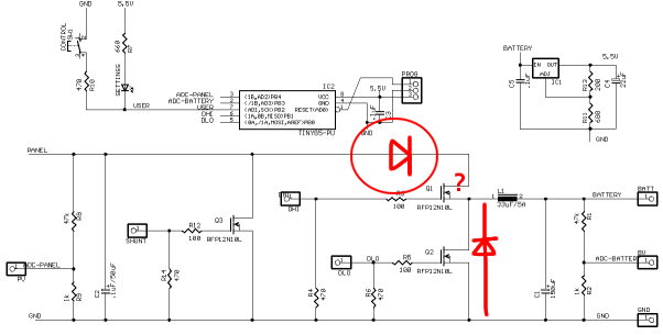
The high and low side FETs for conversion are on the right. Since I want this to be a charge regulator as well, I've put a FET on the left to short the panel when the batteries are charged.
The micro has complementary PWM outputs with dead band timing generation to make sure that both FETs are synchronized; this seems to be a requirement but I haven't found anything that tells me how long the dead band should be? I think I can do multiples of about 20 nanoseconds. I'm guessing that I need a deadband that insures that the turn-off delay and turn-off time finishes before the turn-on delay finishes plus, perhaps, a little bit more for safety?
If I read correctly, I can use either a P-channel or N-channel FET on the high side. Right now I have it drawn as a N-FET but I've noticed that shorting the panel shorts the battery too. I can throw a diode up top but that seems like wasting power.
I've never used a P-FET in my life but it seems to be the opposite of an N-FET and I'd need to change the pull-down on the gate to a pull-up?
I'd like to handle an input of 4 amps and 100v; 100v so that it can handle the Voc of four 12 volt panels. I'm hard pressed to find a logic level P-FET that can meet those specs. But does it have to? ... Isn't the max voltage across the high side Voc - Vbattery? It might be easier looking for a 80 volt part. I can do the math of loss across a diode's Vf vs. a P-FETs Rdson and realize that the P-FET is only a marginal winner over an N-FET and diode. (That assumes that I really can use and N-channel FET on the high side?)
Hm... I think the issue goes away with a diversion load instead of shorting the panel but I'd like the option of not using a diversion load.
Occasionally, I've seen a schottky diode inserted across the low-side FET without explanation. Is that a snubber or is it part of the rectification? ... it just seems a little strange to me since I put the FET on the low side just to get rid of diode in exactly that position!
Comments, help and pointers are greatly appreciated!
- Ed.
